Lithography in microfluidics chip
This was my master’s thesis. The objectives of the project were:
- to build an instrument for photolithography in microfluidics;
- to perform photolithography within microfluidic channels;
- characterize hydrogel
- to culture cells inside the microfluidic system. However, this objective was not completed at the time I submitted my thesis.
In this article, I will introduce the first two points. The third point, regarding hydrogel, will be covered in the biotechnique section, where there is a dedicated article. The fourth point will not be discussed as it was not achieved.
The principle of photolithography in microfluidics is straightforward. A UV source is collimated by a convex lens, and the collimated UV light passes through a photomask that contains the desired 2D pattern. The UV light then illuminates the hydrogel precursor filled in the microfluidic channel through a glass substrate. The hydrogel polymerizes upon exposure to UV, forming a hydrogel structure with the designated shape. Subsequently, PBS solution or water is flushed through the channel to remove unpolymerized hydrogel precursors.
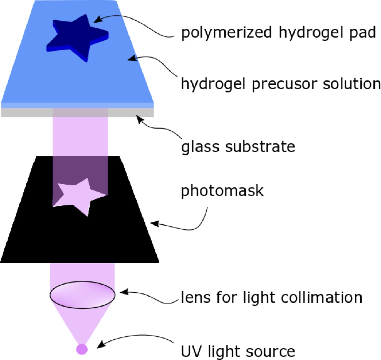
Figure 1: Schematic illustration of the photolithography process in a microfluidic channel.
Instrument
The first stage of the project was to build the photolithography instrument, which was designed based on three main units: the imaging unit, the microfluidics unit, and the UV illumination unit. The imaging unit enables observation during lithography and captures images or video. It consists of a CCD camera, lens tubes for magnification, and a white light source for illumination. The microfluidics unit is a static component designed to hold the microfluidic chips in place. The UV unit provides UV illumination. It consists of a UV LED, a collimating lens, a 3D-printed photomask holder, and a 4-axis stage (X-Y-Z linear stages and a rotary stage).
In addition to the mechanical components, the system includes electronic control components that regulate UV illumination via a Bluetooth receiver. Illumination parameters, including intensity and exposure time, are sent from a mobile device to the Bluetooth receiver, and an Arduino processes the signals between the receiver and the UV LED. The figure below shows the assembled components, both as a schematic design and as the real instrument:
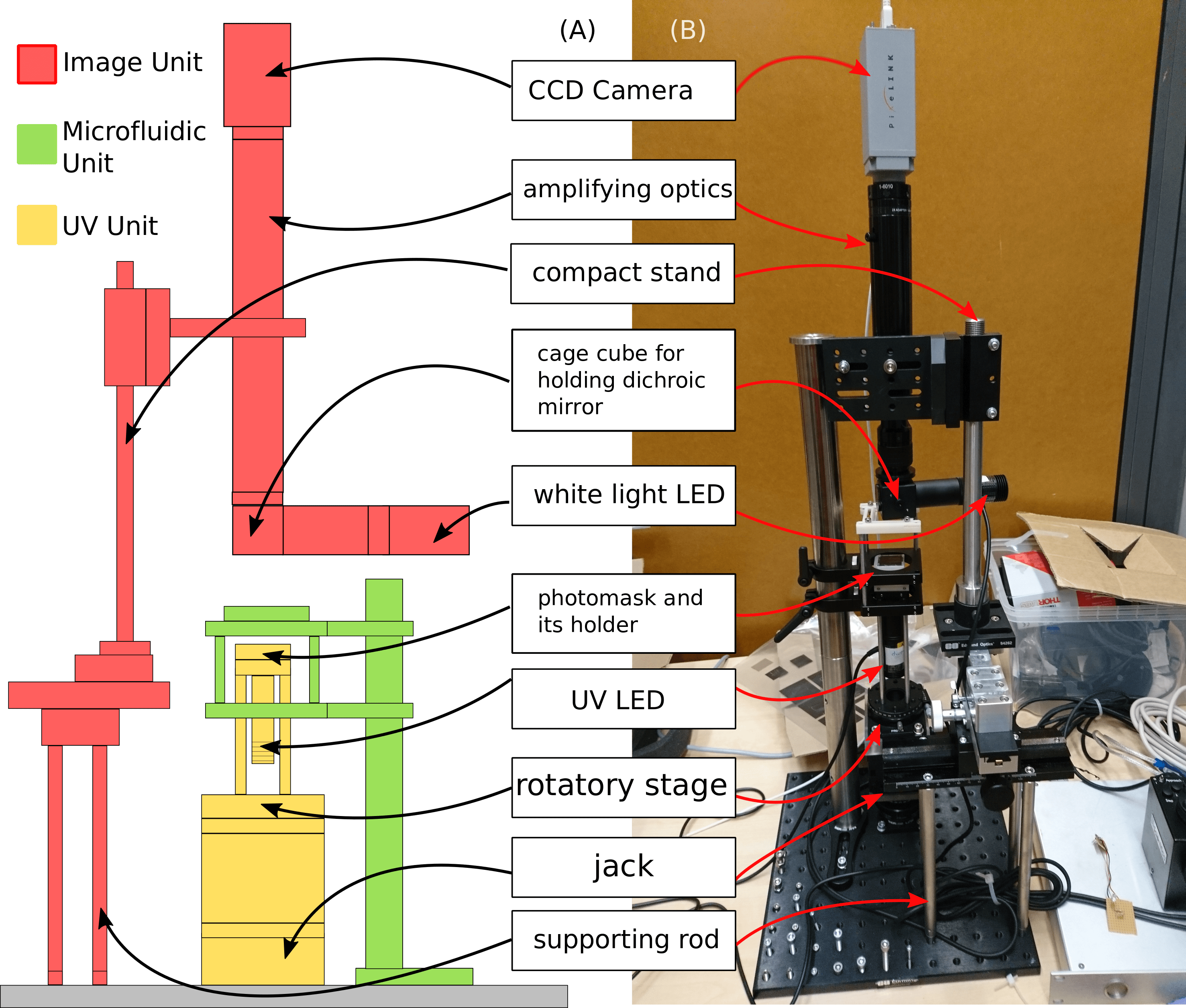
Figure 2: Conceptual design and assembled photolithography instrument.
The instrument operates in conjunction with an external PC for monitoring the microfluidic channels and is paired with a 3-axis external stage controller:
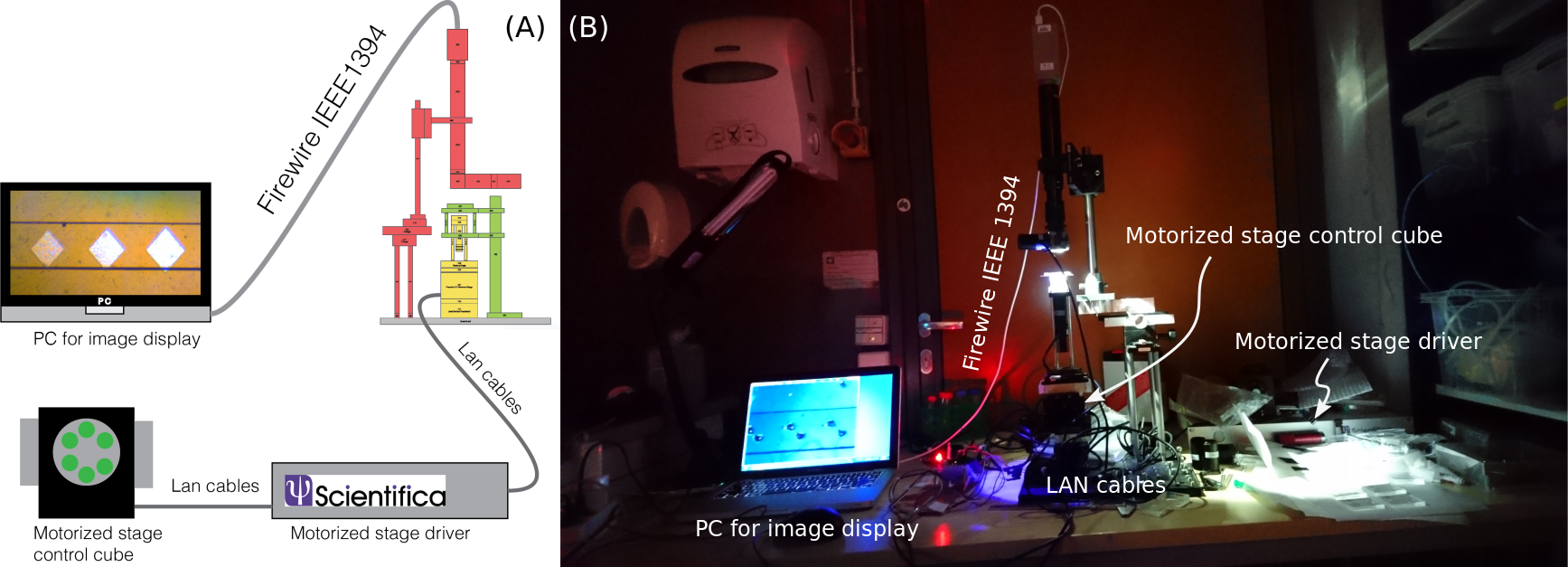
Figure 3: System schematic showing integration of instrument, control, and monitoring components.
Microfluidics
Three microfluidic chips were designed:
- The first chip (left) is the simplest, consisting of 7 channels. Hydrogel polymerization occurs within the channels, serving to validate the principle of on-chip photolithography.
- The second chip (middle), designed by a visiting PhD student, has 8 channels, each containing 8 round chambers with a central pillar. This chip was intended for cell culture using polymerized hydrogel, but the small channel dimensions limited its practical use.
- The third chip (right) is a modified version of the visiting PhD student’s design, with larger chambers and channels, as well as valves to control fluid flow. It was not used in the master thesis experiments (as the first chip was sufficient), but it is intended for future applications. The images of these three microfluidic chips are shown below:
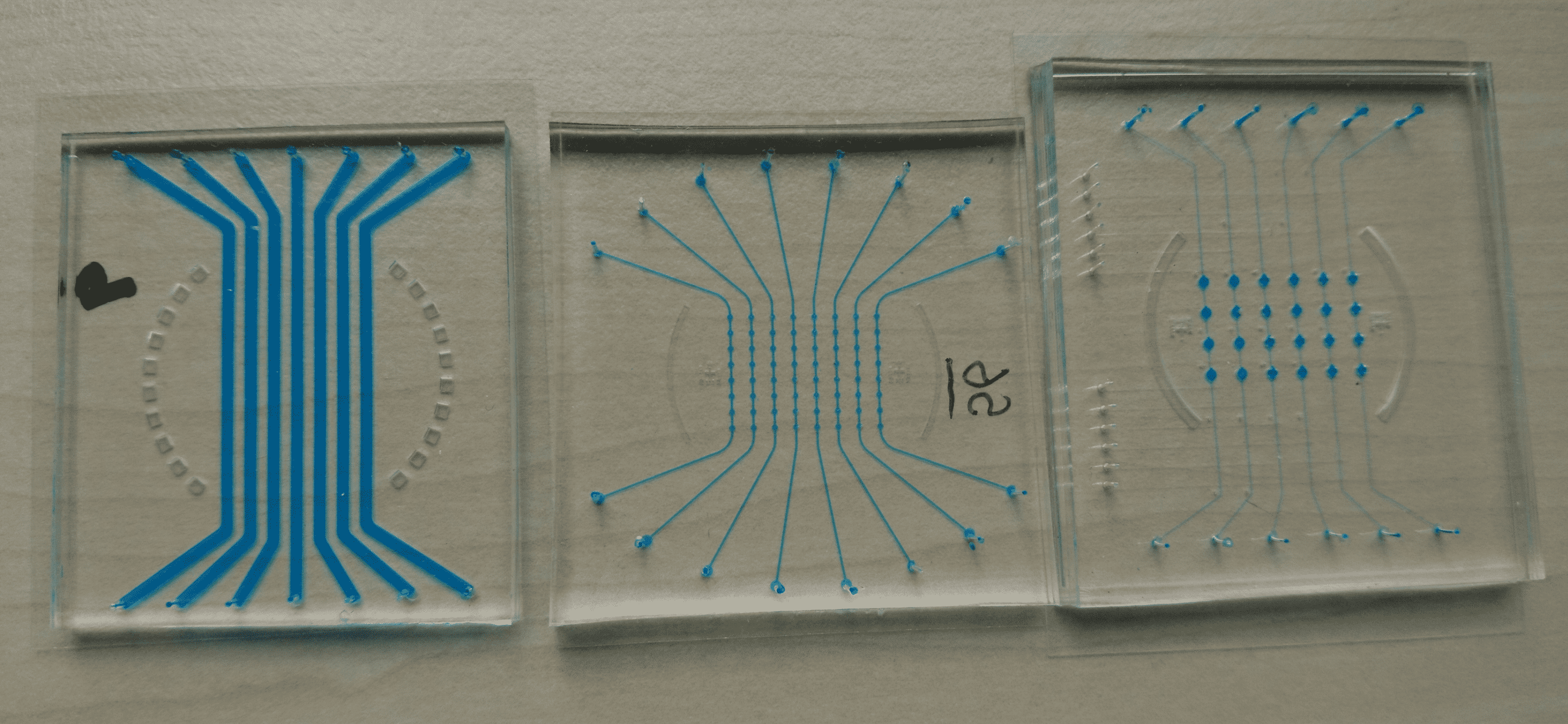
Figure 4: Three generations of microfluidic chip designs used for on-chip photolithography.
Lithography on a Chip
Photomasks of varying shapes and sizes (800 µm to 30 µm) were designed to test the resolution of on-chip photolithography. The smallest achievable pattern was ~100 µm.
Hydrogel structures with diamond shapes were stained with trypan blue for visualization, and excess dye was washed away with PBS:
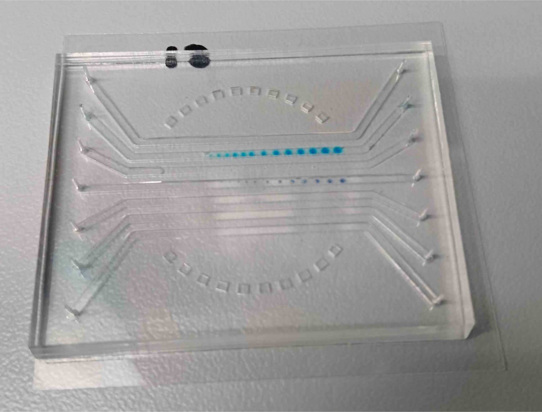
Figure 5: Diamond-shaped hydrogel patterns visualized using trypan blue staining.
Resolution testing was conducted by varying the GelMA DoF and photo-initiator concentration. A higher photo-initiator concentration (1%) enabled the formation of smaller features (14 patterns in 300 s), while a lower concentration (0.5%) yielded only 10 patterns.
The following shows examples of hydrogel patterns formed in microfluidic channels. All channels were filled with PBS except the rightmost channel, which contained air:
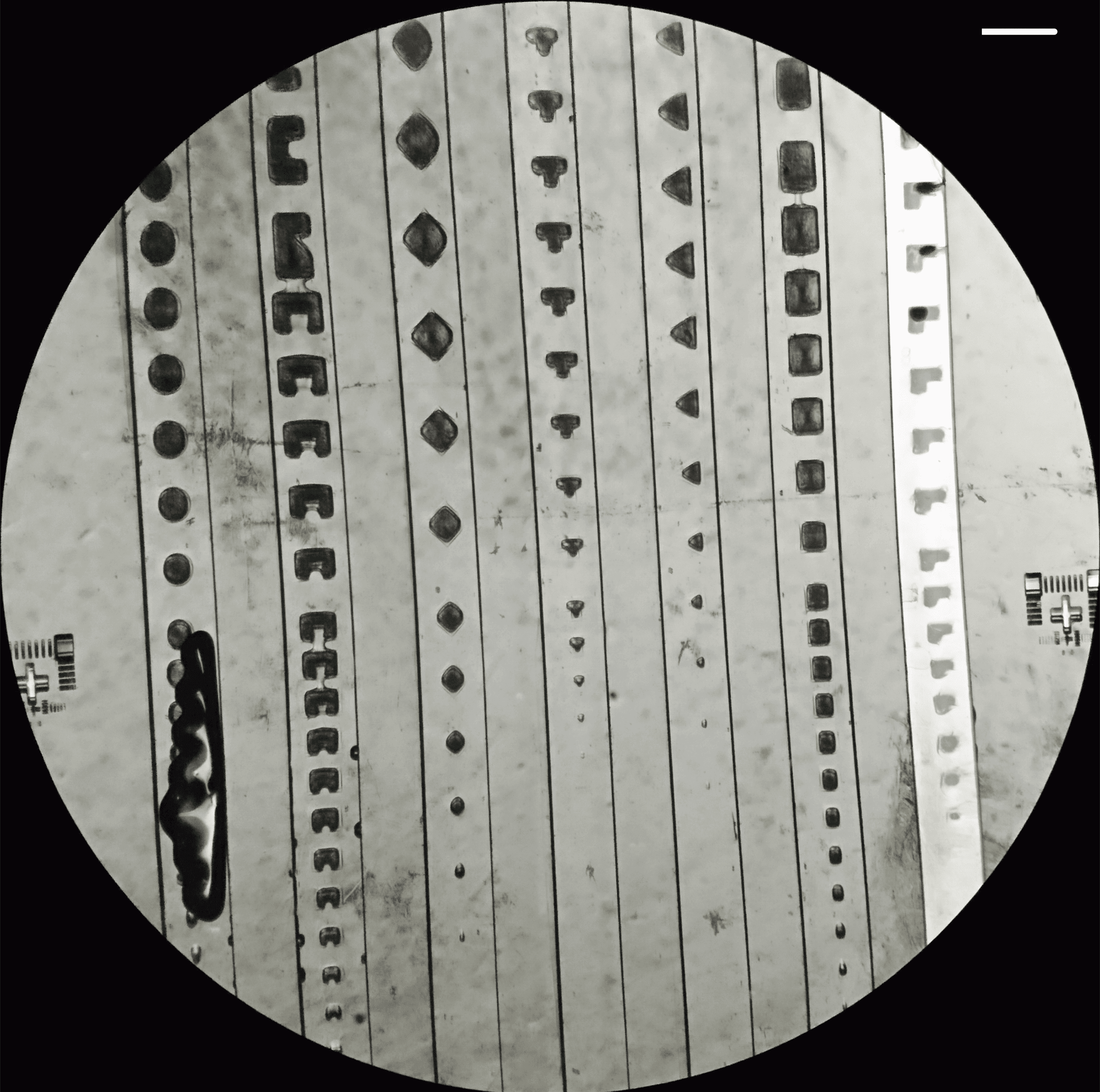
Figure 6: Hydrogel patterns formed within microfluidic channels under different filling conditions.
Some defects were observed: hydrogel structures deformed after flushing, likely due to swelling and fluid pressure:
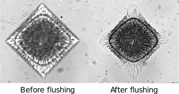
Figure 7: Deformation of hydrogel patterns after հեղushing due to swelling and pressure effects.
Unwanted polymerization occurred, especially for concave shapes, likely due to UV scattering:
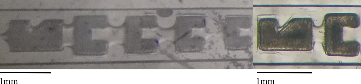
Figure 8: Unintended polymerization effects observed in concave geometries due to UV scattering.