Lithography in microfluidics chip
This was my master thesis. The target of the project is 1) to build an instrument for photo-lithography in microfluidics; 2) to make photo-lithographies inside microfluidics; 3) to culture cell within microfluidics.
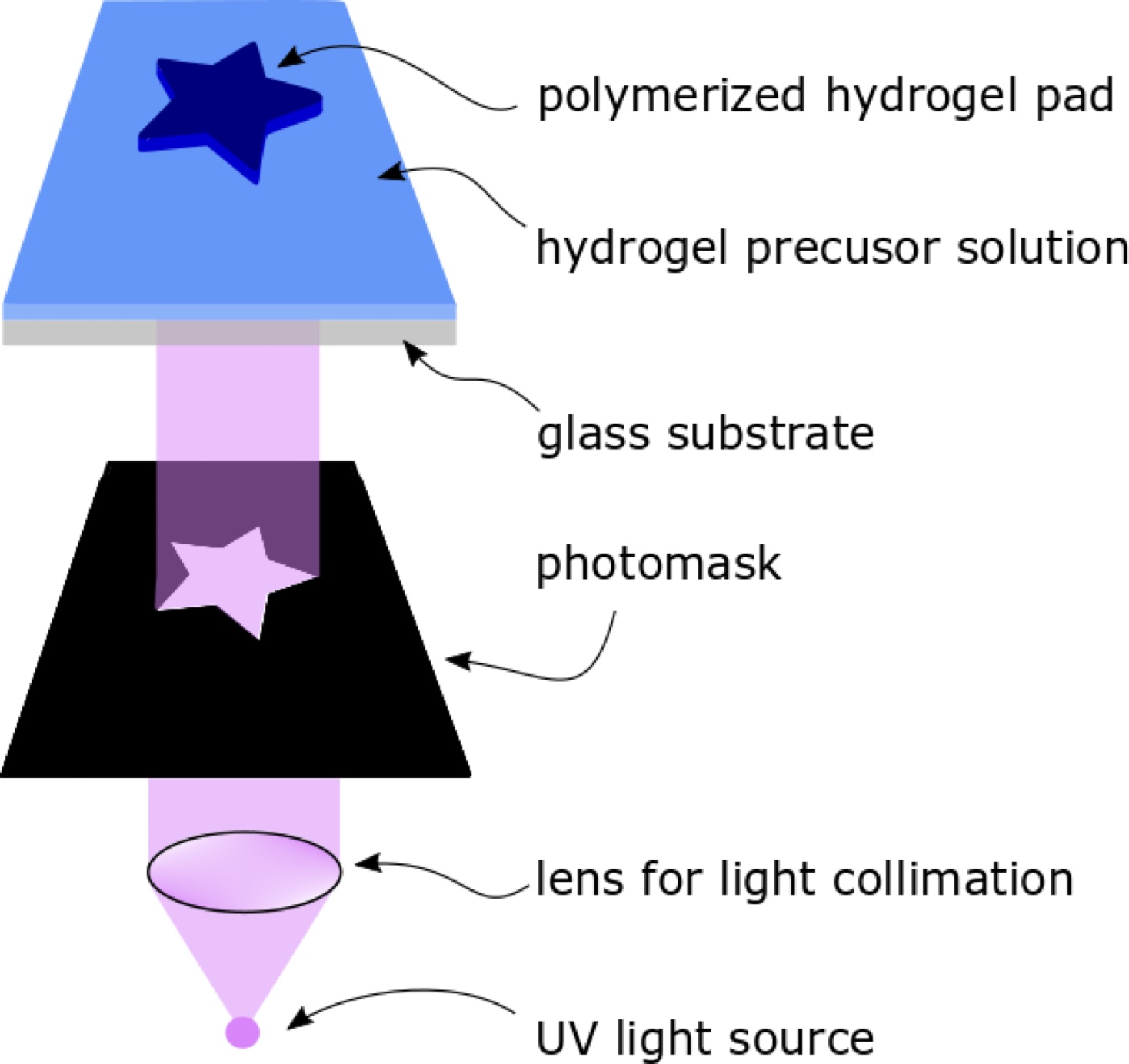
The principle of photo-lithography in microfluidics is not difficult to understand. There is a UV source, that will be collimated by a convex lens. The collimated UV is then pass through a photomask, that gives a 2D pattern, which we want. After that, the UV will be shotted through the glass substrate and into the microfluidic channel, where hydrogel precusors were filled. The hydrogel starts to polymerize, once UV was reached, and in the end, a hydrogel pad with a designated shape will be formed. After that, PBS solution or water can be flushed in order to remove unpolymerized hydrogel precusors.
Instrument
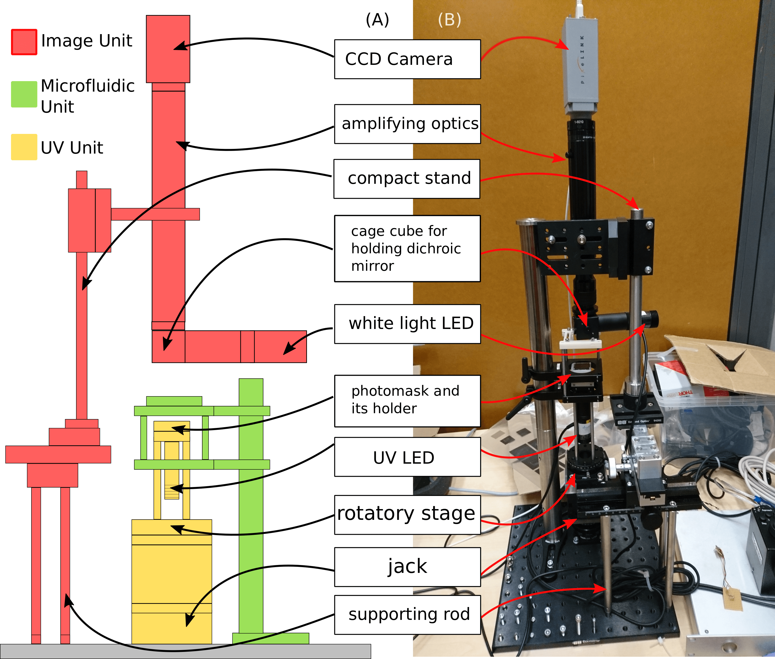
The first stage is to build an instrument for photo-lithography. This instrument was built based on … . There are three units: image unit, microfluidics unit, and UV unit.
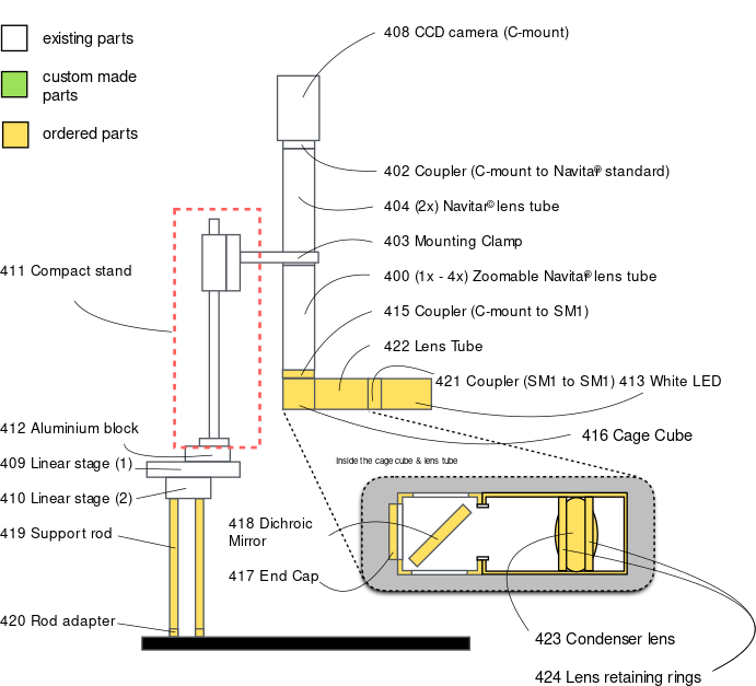
The image unit is for taking video/images, and observation during lithography. It consists of a CCD camera, lens tubes, which were for amplification, and a white light source, which served as an illumination for microscopy. The design of the image unit is shown below.
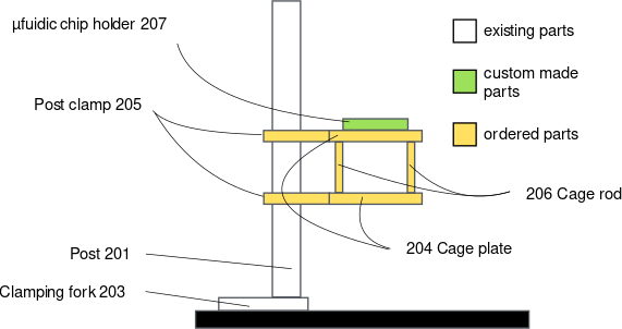
The microfluidics unit is for holding microfluidics. It is solely a static component.
The UV unit is for illuminating UVs. There are UV LED, lens which collimates UV light, and a photomask holder, which was 3D printed and for holding a photomask, and a 4-axis stage, x-y-z stage and a rotatory stage.
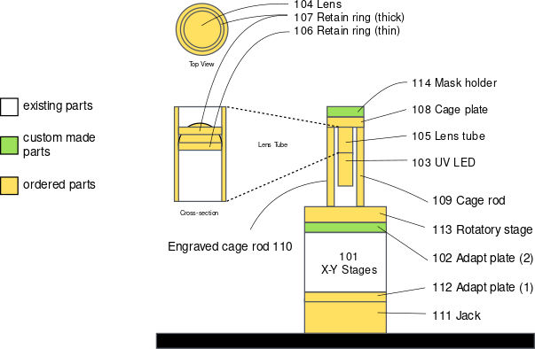
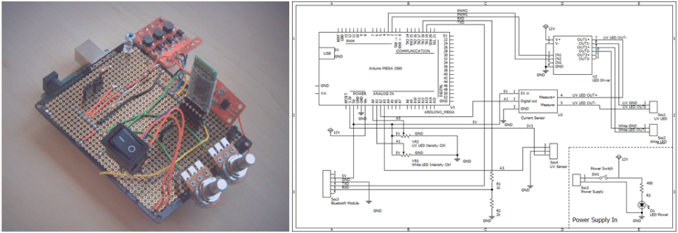
Beside to mechanical parts, there is also electronics, which controls UV illuminations with an bluetooth receiver. So the illumination command, including the intensity and time, was sent by a mobile device, which was connecting to the bluetooth receiver. An Arduino was used for processing the signals in between bluetooth receiver and UV LED.
By the way, this figure shows all the assembled components, in schematic design and real instrument.
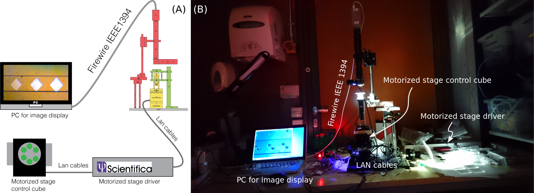
The instrument is not supposed to work independently, but also with an external PC, which observes the situation in microfluidics, and an external stage controller, which was provided by scientifica.
Microfluidics
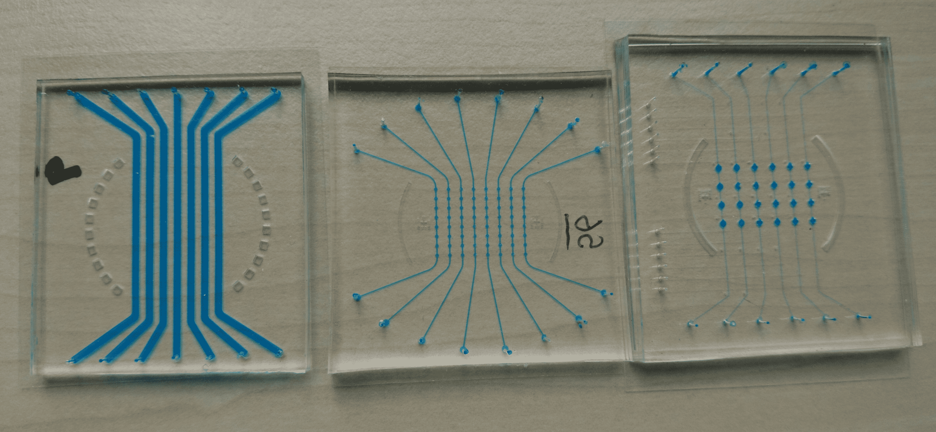
Three microfluidic chips were designed. The first chip (left) is mostly used, and simplest among all. It consists of only 7 channels. So the hydrogel can be polymerized within the channel. This chip is to prove the principle of photo-lithography on a chip.
The second chip (middle) is designed by Stephen, who were the visiting PhD student. There are 8 channels. Each channel consists 8 round chambers, and in the center of each chamber there is a round pillar. This chip is designed for creating cell cultures using polymerized hydrogel in each chamber. In the end, it is not utilized widely, because the dimension of the channels is too small, which is not facilitating the polymerization on a chip.
The third chip (right) is a modified version toward the Stephen’s chip. It has larger chamber and channel size. It has also the valves, which controls the close or open of the microfluidic channel. It is not used, because the first chip is enough to handle all the experiments for my master thesis, and it is supposed to be used for future…
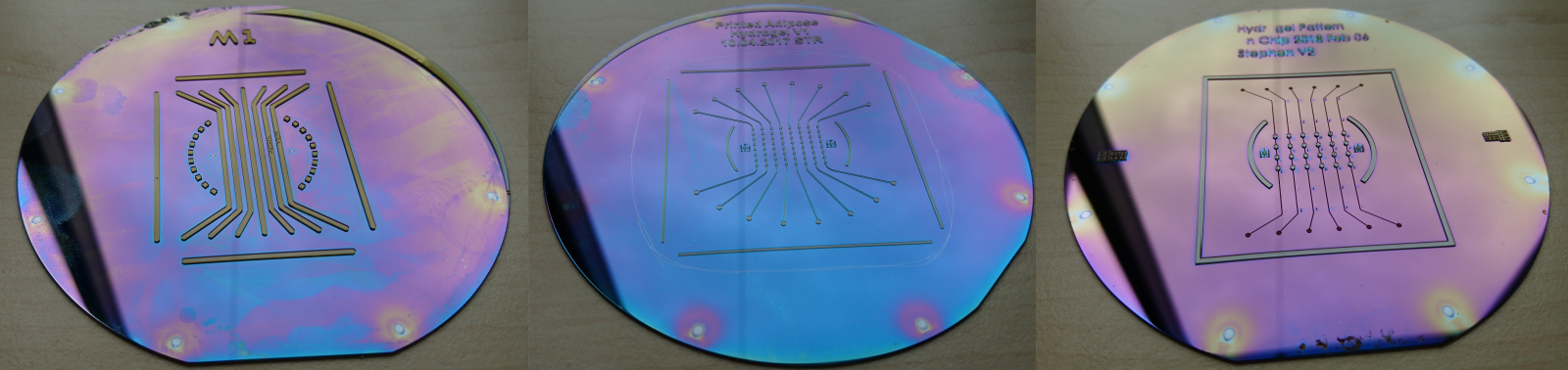
Microfluidics was fabricated via soft-lithography. A silicon wafer will be pre-fabricated, which served as a mold. The figure below displays the wafers used for fabricating the chips above.
Hydrogels
Hydrogel is a bio-compatible material, which is used as the resin for photolithography on a chip. Normally, the hydrogel is fabricated in liquid state, which consists of lots of monomer, which has vast double bonds. Once the photo-initiator react with the monomer, it starts to form polymer with other monomers. And it is a chain reaction, therefore, a very long polymer could be formed in the end. Many polymers form meshwork structures, which was the essence of polymerized hydrogel. The polymerized hydrogel can be absorbed by water, that was called swelled state.
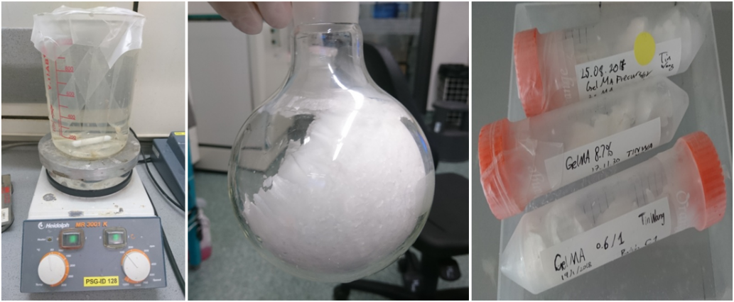
Here I have used the photo-polymerizable hydrogel, which modified from gelatin, called Gelatin methacryloyl (GelMA), for the photo-lithography experiments. It takes 7 days to fabricate one batch of GelMA. Basically, the fabricating procedure is to dissolve gelatin into water, add methacrylic anhydride into gelatin solution, a chemical phenomenon called “graft” will happen, that will replace the amine group originally within gelatin molecules, and then dialysis the 7 days. The dialysis is to remove the unreacted methacrylic anhydride, which is toxic. The dialysis is shown in the left figure below. For better storage, the GelMA precusory will be freeze-dried. The middle figure is shown the freeze-dried GelMA. The right figure shows the way to store the GelMA, which was frozen under -20°C.
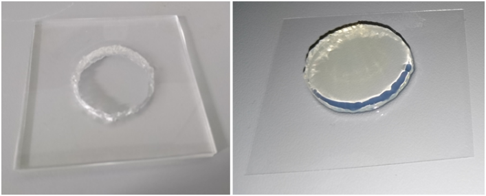
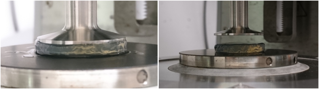
I used rheometer to characterize its mechanical property, specifically the storage and loss modulus. Before the measurement, I have produced a hydrogel pad, which is in round shape (right). There is a PDMS mold, which holds a 2ml GelMA precursor (left). It polymerized once UV is illuminated.
The pad is directly placed under the probe of rheometer. The probe will touch the hydrogel pad, and give around 1N force toward the hydrogel. The measured programe was programmed by other staff in the lab. Basically, the probe rotates and stops with a specificed frequence. It measures how the probes reacted to a given rotatory force, which is the storage modulus, and how it behaves when the probe suddenly stops, which is the loss modulus.
The storage modulus is considered, because the loss modulus signal is not stable, and flucating all the time. I have measured the storage modulus with same batch GelMA but different concentration in its precursor. Obviously, the highest concentrated GelMA gives the highest storage modulus. And the lowest was the 5%.
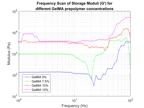
The storage modulus below 10 Hz is quite stable, which is called plateau modulus. I have measured the plateau modulus for the 4 types of concentration for 4 times. And summaried the data below. In general, it gives that the plateau modulus is positively proportional to its concentration.

Apart from the mechanical property, there is also a property called degree of functionality (DoF). Since the GelMA was formed by grafting, where the methacrylic anhydride molecule was replaced the amine group, which was originally in the molecule of Gelatin. The DoF counts the percentage of amine group, which was replaced by the methacrylic anhydride.
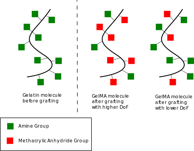
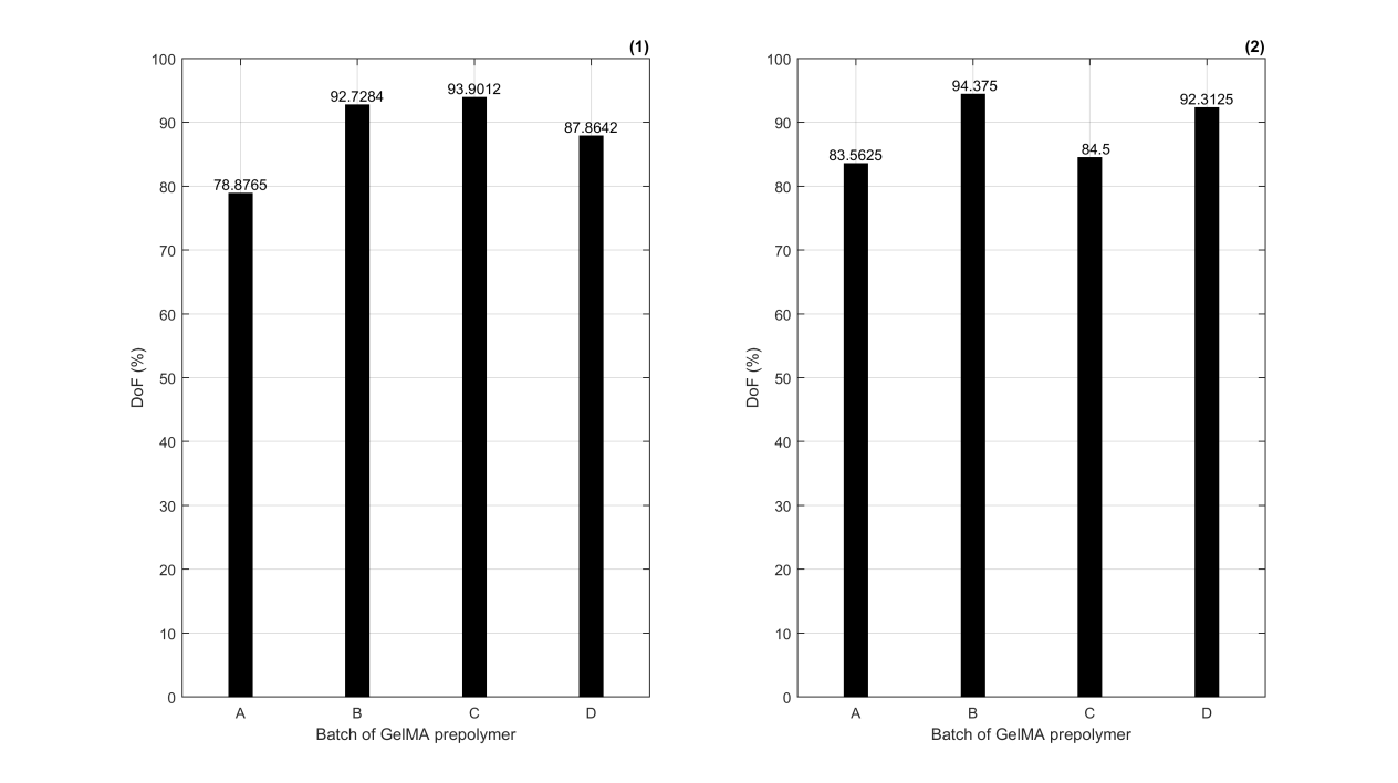
The DoF was measured by ninhydrin assay, which measures the amount of amine group in the molecule of GelMA molecules. The DoF is supposed to be controlled by the amount of methacrylic anhydride added into the gelatin solution. Here I have prepared 4 batches of GelMA, with different amount of methacrylic anhydride added, 1.2, 0.8, 0.6, and 1.2 gram of methacrylic anhydrided added per each gram of gelatin, corresponding to batch A, B, C, and D. I have measured the DoF for each batch twice, the result is quite out of expectation (figure below). So that the DoF is high for all batches (>80%), that indicates even 0.6 gram of methacrylic anhydride is already a lot for synthesis GelMA.
Lithography on a chip
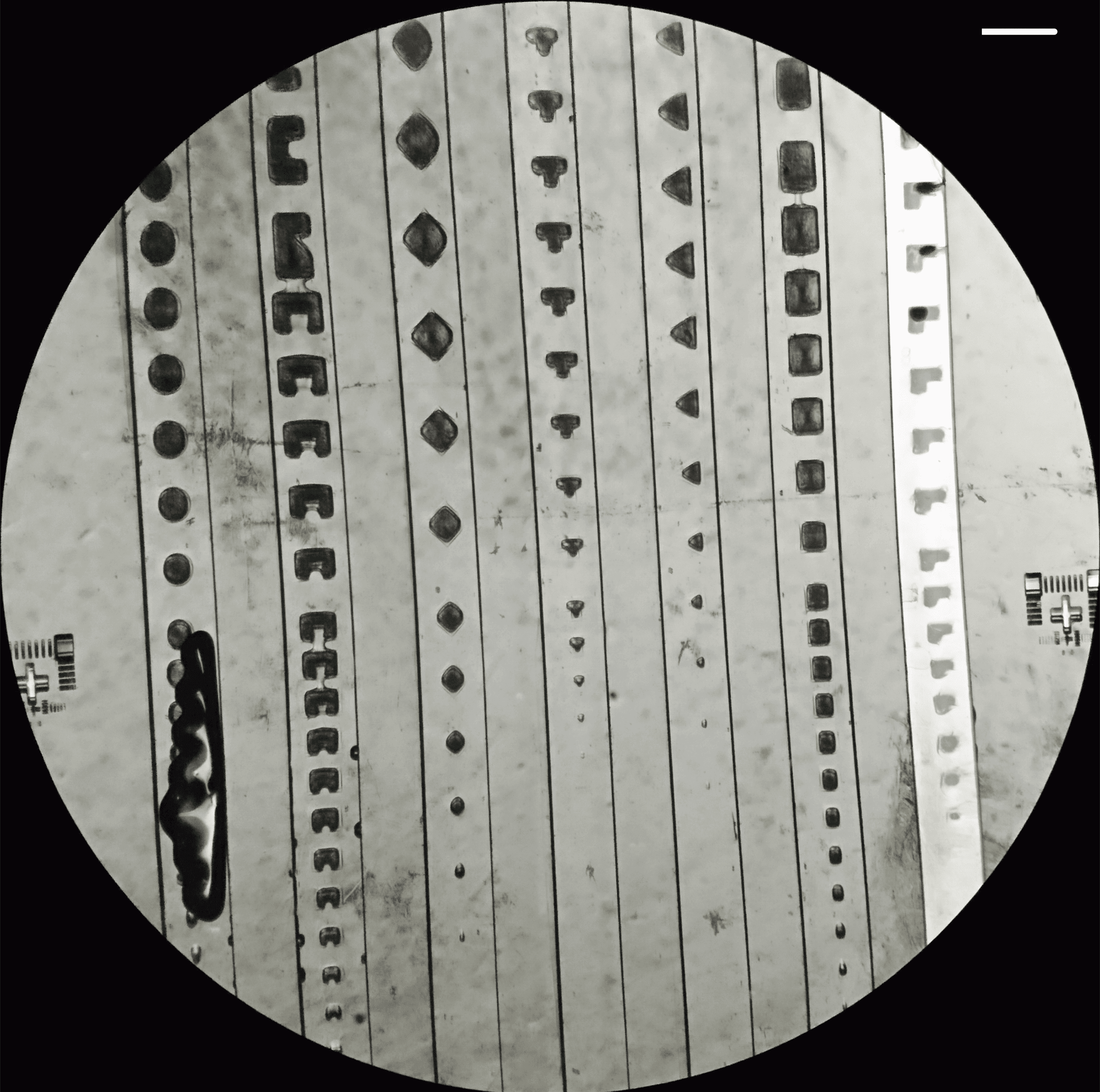
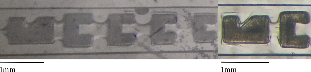
I have design different photomask, the one mostly used is that with different shapes and varying its size from 800 um to 30 um (figure below). It tests the resolution of the on chip photo-lithography which is possibly to be reached. The smallest possible pattern is around 100 um.
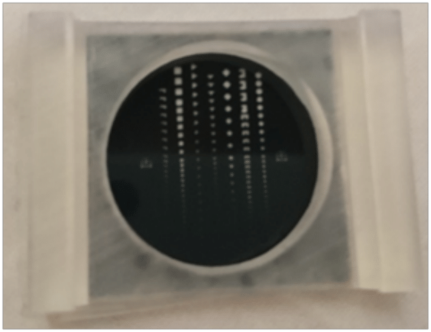
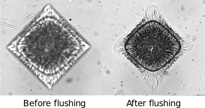
For display purpose, I have stained the polymerized hydrogel pad with diamond shape by using trypan blue (figure below). Once the hydrogel is stained, it will be washed by PBS solution.
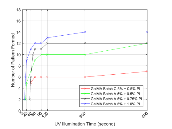
To test its smallest possible pattern could be formed, I used different DoF of GelMA and different concentration of photo-initiator. The figure below shows the number of pattern it can be formed with respect to the UV illumination time. The higher number of pattern can be formed means the smaller pattern can be patterned or higher resolution can be reached, because the photomask size is declining with increasing the pattern number. Obviously, higher concentration of photo-initiator (1%) gives better resolution of pattern (14 patterns) under 300 seconds of UV illumination. Comparatively, the photo-initiator 0.5% gives only 10 patterns.
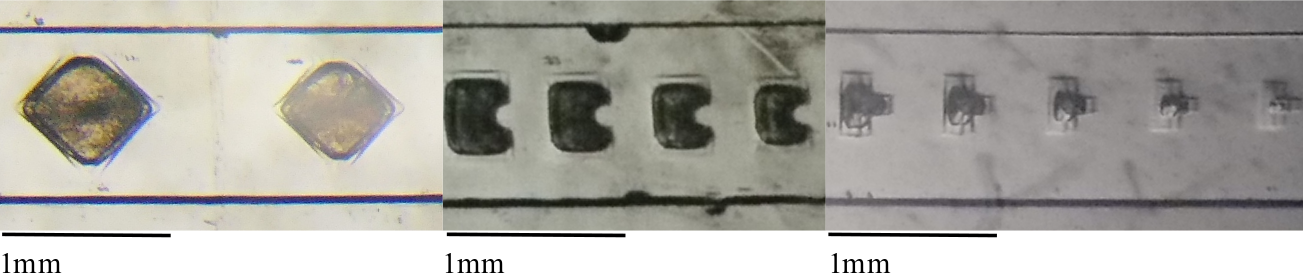
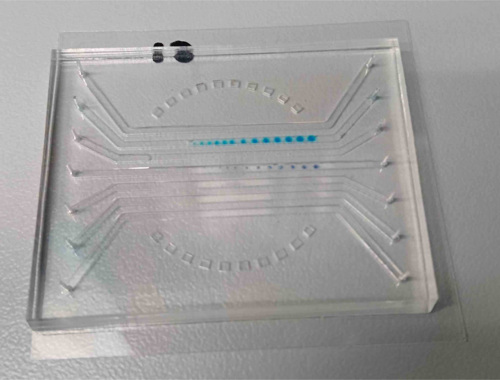
The figure below shows the pads patterned using the photomask above. All channels with the pads are filled by PBS solution except the right most channel, which was only filled by air.
The on chip photo-lithography is not ideal, therefore, some defects were observed. Firstly, the pads will deform, once PBS solution or water was flushed through the channel. That is probably due to swelling to hydrogel. And also, the flushing pressure could damage the pattern.
Moreover, there are also unwanted polymerzation. It was observed during the patterning of 凹-shape. Figure below shows there are many connections between the pads. That could be due to the scattering of UV within the GelMA precusor.
Furthermore, it found that the pattern inside channel is uneven distributed. That means the surface of the pattern is not flat, but with a curved shape. I guess that is because the polymerization starts from the middle of the hole of photomask. Therefore, the middle part is the highest.